BACKEND DESIGN SERVICE WORKING FLOW
Design Input:
- Netlist
- CPF/UPF
- SDC
- Clock structure
- Dataflow
- IO table
DFT:
- Stuck-at test(cov: >97%)
- Full at-speed Scan Test (cov: >75%)
- Full at-speed Memory BIST test
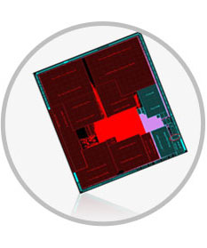
Floorplan:
- Memories
- Multiple power domains division
- Physical cells
- MTCMOS
- Power plan
Placement:
- Scan Reorder
- Timing-driven placement
CTS:
- Clock Skew and latency optimization
- First function clocks, then DFT clocks
- Scan reorder
Routing:
- Optimize VIA
- Timing Optimize
- Crosstalk Optimize
Timing Closure:
- Leakage optimize
- Clocktree ECO
- Critical Path double space 、double width
- Reduce Noise
Physical Verification:
Design Output:
- GDS
- Provide reports:
- Timing
- IR
- PV reports
- ATPG database